India's semiconductor strategy: mature nodes and packaging
LeadPrelims and MainsJune 2026
Why in news
NITI Aayog's Frontier Tech Hub has released a report, Future of India's Semiconductor Industry, reported on 3 June 2026. It advises India to put public money into mature chips and packaging, and not into the most advanced chips.
Background
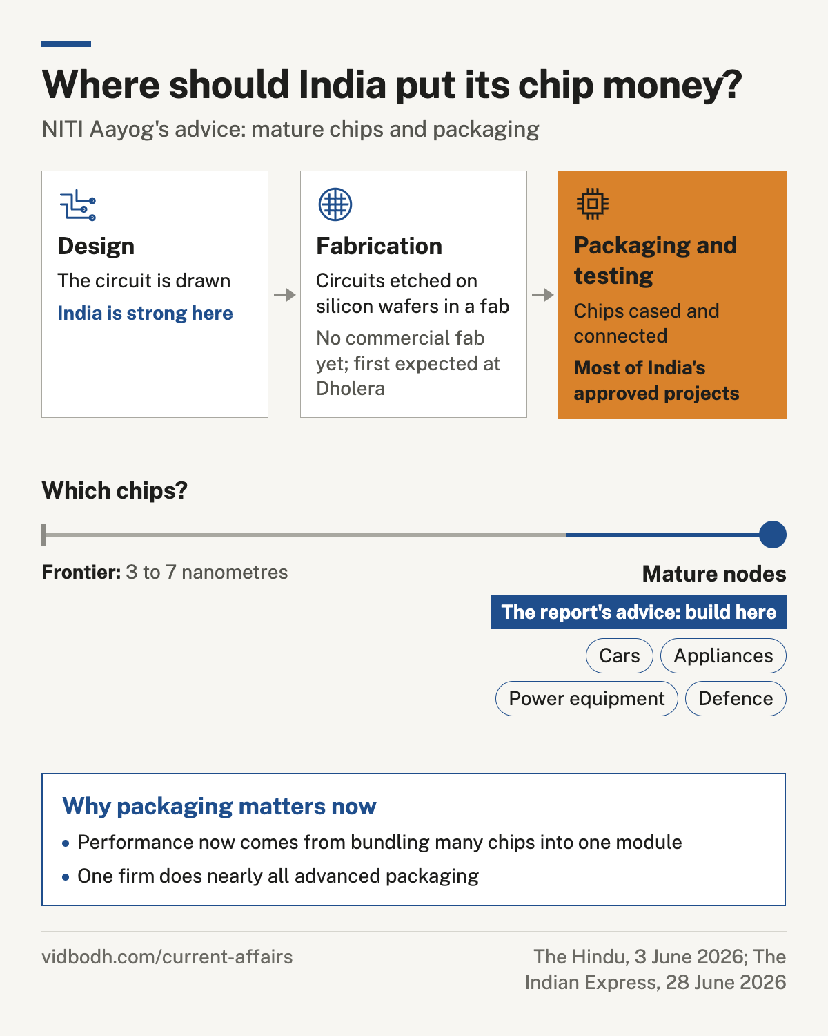
- A semiconductor chip is made in three stages: design, fabrication and packaging and testing.
- Fabrication happens in a fab, which etches circuits on silicon wafers. A fab takes four to five years to start production and needs costly imported equipment.
- A chip's node, measured in nanometres, describes how small its features are. A smaller node means a more advanced chip.
- Mature nodes are older and larger. They run cars, appliances, power equipment and defence systems.
- India is strong in design and has no commercial fab yet; the first is expected at Dholera in Gujarat.
What the report says
- India's ecosystem cannot yet meet demand, but manufacturing must be pursued for national security.
- Do not chase the frontier of 3 to 7 nanometres; build mature and compound semiconductor capacity.
- Treat packaging as a core pillar.
- Work with partners: the United States, Japan, the European Union and South Korea.
- The idea is selective depth: be strong in chosen parts of the chain and not copy all of it.
Why packaging matters now
- Packaging places the bare chip in a protective case with connectors.
- As shrinking transistors gets harder, performance comes from bundling many chips into one module. This is advanced packaging.
- One Taiwanese firm does nearly all of it, and supply is short of demand: a choke point for artificial intelligence chips.
- High bandwidth memory, stacked memory used with these chips, is in such demand that ordinary memory prices have more than tripled, raising the cost of phones and computers.
What it means for India
- Most of India's approved projects are assembly, testing and packaging units, which matches the report's advice.
- Packaging needs less capital than a fab and builds skills that lead upstream.
- Dependence on a few suppliers is a risk for every country, as the memory shortage shows.
The way forward
- Fund mature node fabs for the chips India uses most.
- Build advanced packaging capacity and the skills for it.
- Support design firms, where India already has talent, to own their intellectual property.
- Secure equipment and materials through partnerships.
Prelims facts
- The chip chain: design, fabrication, packaging and testing.
- A smaller node means a more advanced chip.
- India's first fab is expected at Dholera, Gujarat.
- CoWoS, chip on wafer on substrate, is an advanced packaging technology.
See also: Advanced packaging: the CoWoS chokepoint · High bandwidth memory · Semicon India Programme
Sources: The Hindu, 3 Jun 2026: The future of India's chip industry (opens in a new tab) · The Indian Express, 28 Jun 2026: How a niche technology became a choke point for AI (opens in a new tab) · The Indian Express, 12 Jun 2026: More expensive phones, PCs: How consumers are paying for the AI boom (opens in a new tab) · The Indian Express, 14 Jun 2026: Memory chip shortage, electronics price rise, inflation (opens in a new tab) · PIB, 27 Jun 2026: Digital India Nears 11 Years, Driving India's Next Phase of Technology-Led Growth through Artificial Intelligence, Semiconductor Manufacturing, Digital Public Infrastructure and Affordable Digital Connectivity (opens in a new tab)
Earlier coverage: The future of India's semiconductor industry · The monthly magazine, June 2026